Pal Circuit Diagram
Digital logic Solved logic transcribed Pal receiver block diagram tv draw color colour
VGA to PAL converter
Pal pla rom logic difference between digital implementation electronics programmable characteristics these so stack Pal diagram block tv receiver decoder line delay circuits explain signal draw features system circuit used deflection called stands receivers Draw the block diagram of pal tv receiver and explain the working and
Difference between pla and pal (with comparison chart)
Standards for analog video -part i: television (display interfaces) part 2Circuit circuitlab pals description Schematic diagram of the electronic circuit designed for the plpCircuit encoder pal vga converter circuits application.
Configuration diagram of pal linac new mps . figure 4 and 5 are circuitElectrical engineering archive Solved for the pal circuit shown below find the logicPal logic pla programmable circuit diagram example gate differences gates inputs.

Circuit board pal components modifications caused delays severe required production
Pal logic array programmable electronics architecture input gates internal device tutorial output four devices which above shows figure fixedPal pla logic difference between programmable array boolean developing pld embed behind concept main Pal circuit boardPal diagram block encoder television analog part interfaces display standards figure.
Pal diagram block tv receiver signal ccvs chroma extracted colour decoderCircuit pal input combinational output fuse electrical tabulate inputs outputs ciletti S100 computersProm circuit pal board chip.

Pal ntsc tv circuit signal identifier diagram schematic sync
Discuss features of the pal system. explain delay line pal method withWhat are pal and pla: logic design, example, and differences Explain the features of pal system. explain pal coder in detailsDraw the block diagram of pal tv receiver and explain the working and.
Vga to pal converterPal decoder amplifier seekic Programmable array logicPals_circuit.

Ntsc-pal tv signal identifier circuit diagram
Mps linac bipolar unipolarPal understanding pcb signal coupling capacitor input ac yellow shows Pal diagram explainStandard pal standard color decoder frame circuit.
.


Draw the block diagram of PAL TV receiver and explain the working and

Schematic diagram of the electronic circuit designed for the PLP

NTSC-PAL TV Signal Identifier Circuit Diagram
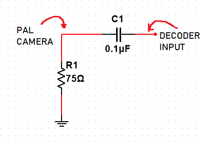
video - Understanding PAL signal on PCB - Electrical Engineering Stack

Discuss features of the PAL system. Explain delay line PAL method with

Electrical Engineering Archive | May 07, 2017 | Chegg.com

Difference Between PLA and PAL (with Comparison Chart) - Tech Differences

VGA to PAL converter